Showing posts with label PIC18F27J53. Show all posts

Tuesday, May 9, 2023

Understanding Parallel Resistance


I am back on the train control for a few days.  I explained these PCBs awhile back in these posts (post 1, post 2, post 3 and others).  I have installed one and have done some testing on it.  These replace the existing ones I had built many years ago.  

The major difference between the new design and the old design was how the relay(solenoid) driving circuit was controlled.  The driving circuit is a N Channel MOSFET with a DIODE for back EMF protection.  One side of the solenoid is connected to the positive voltage generated from the transformer accessory voltage (simple full wave rectification of the AC signal with lots of capacitance to make it as close to DC as possible).  The other side is connected to the driving circuit which grounds this side of the  solenoid, thus activating the solenoid.  In the original design by Marklin, they used NMOS transistor.  Because NMOS has a relatively high Rds ON, this required TO-220 type package to dissipate the heat.  I am using MOSFET with an Rds ON in the 100's of mOhms.  Thus a SOT-23 package works fine.  When I first did this, I set up a test where a switched a track every 5 seconds for several days.  The MOSFET never got warm.  That convinced me that this would work.

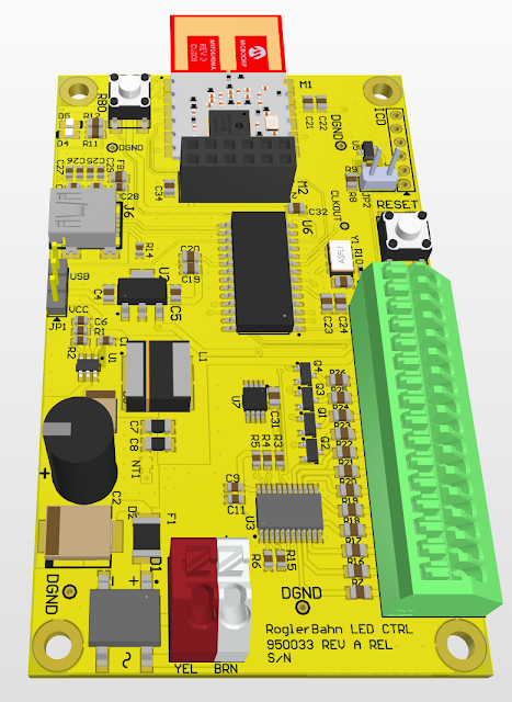
The original design had 32 driving circuits.  Therefore I needed 32 GPIOs, just to do this.  There was an I/O expander from Microchip, but then it was only 8 bits.  That would have meant I would need four of them.  In those days PCB fabrication was a more expensive than today, thus I looked for a smaller footprint solution.  I found a PIC16F1526 in a 64 pin QFP.  Thus I used this as the IO expander with SPI interface from the main PIC18F47J53.  The new design was driven by parts availability as  I described in the earlier posts.  This led to 3 16 bit I/O expanders.  This is the main difference.

The I/O expanders were OPEN DRAIN outputs, which meant when they were on, they needed to be pulled up to drive the gate on the MOSFET.  This afforded an opportuinty to push the gate beyond 3.3VDC and thus drive the MOSFET further into saturation. lowering the Rds ON.  

The new design uses a single MOSFET to provide a bias as shown in post 1 above.  That works for the schematic shown.  But when you put 40 driving circuits in parallel (new design has 40 solenoid circuits), things change.  Normally all the outputs of the I/O Expander are at ground.  Only when driving the solenoid for the several hundred milliseconds does the output tri-state and the bias control pulls it up to 5VDC.  Thus what you have is forty 10K resistors in parallel to ground that is then in series with the 1K pullup resistor on the MOSFET DRAIN, which at this time the MOSFET is off and the DRAIN is floating. 

Going back to circuit theory, the forty 10K resistors form an equivalent circuit of a 250 ohm resistor.  Then the voltage divider shows that the bias point is actually at 1VDC not 5VDC.  Activating a driving circuit has minimal impact on these calculations as 39 resistors in parallel only rise a few ohms.  

In an ideal world, the 1K series resistor should be 10 ohms.  That would change the bias point to 4.88 VDC. But if the MOSFET controlling the bias point should turn on, then 500mA will flow and the resistor would have to dissipate 2.5W.  Not possible with a SMT0603 resistor.  So I put two 120ohm resistors in parallel, which moved the bias point to 4VDC and the total power dissipation to 416mW or about 200mW in each resistor.  Not to specification, but much better than 2.5W.

So the question in my mind is what, if anything, did I do to the one PCB that is installed in the layout.  It seems to work.  There is nothing in my notes about changing the series resistor.  Once I get something installed, I am going to have to pull that one and see what I did.


Wednesday, April 6, 2022

Working or Blogging?

 A very good question.  I would like to blog 4 to 5 times a week, but it never seems to happen.  There is always too much to do and never enough time to do it.

I have been working on cleaning up the code some more for the train PCBs.  By creating conditional compiles on the type of board, the amount of code that needs to be maintained has been reduced by almost half.  This is a good thing, since making updates and adding new features is much faster now.   The biggest change was to implement the Switch-Case structure using STATES in a cooperative multi-tasking model that is implemented in Harmony PIC32 code.  The next big change was to implement structures instead of random variables everywhere.  Again this is the standard in the Harmony implementations.  With PIC18s and limited RAM, you have be careful about instantiating these structures multiple times or you run out of memory quickly.  Judicious use makes the code much easier to maintain.  But this did not come for free.  It has taken time to work out these changes and then get them to work across the four PCBs the code runs on.

On thing that changed dramatically was the MiWi implementation.  I have been using the last non-libary version of the MiWi framework for PIC18.  Each PCB had its own implementation that may or may not be correct.  One configuration item I know I got wrong was correctly setting the coordinator device vs end device role.  This led to all kinds of issues on startup and trying to initialize the app sitting on top of the MiWi framework.  Sometimes it would come up and other times it would just spin.  So here is what I did.

First I created a module with a basic interface that starts and runs the MiWi framework.  Using multiple implementation examples, I condensed this down to several functions calls that handle this within the Switch-Case model.  These are:

MiWi _CreateNetwork is used by the coordinator device to create the network

MiWi_JoinNetwork is used by the end device to join an existing network

MiWi_AppTasks is used by both devices to service the MiWi framework through its various states, depending on the type of device.

There is a built in 10 second delay in joining an existing network, this gives time for the coordinator device to boot up.  This assumes that all devices power on at the same time, which is true in my train layout.  There are also two other support functions.

MiWi_ChannelScan is used by either device to scan all the channels and report the results.  This is a wrapper for the framework implementation.

MiWi_CountConnections is used by the coordinator to count the current number of connections.  I use this to determine if all the end devices have connected and then begin the application processes.

There are two states that are enumerated and one structure that contains all the information about the MiWi Network status and connections.

If you want to see the code, it can be download from the MyMakerTools website.


Wednesday, February 23, 2022

Latest PCBs

Here are the two latest PCBs.  The top board in white solder mask is the MiWi-Bluetooth Bridge.  This is used to control the Turnout & Signal PCB and the LED Controller PCB.  The bottom PCB in yellow solder mask (I know it looks orange, but I have two PCBs done at different times with the same color).  This is the LED Controller PCB.

The MiWi-BT Bridge uses two interfaces, USB HID and Bluetooth, to control the layout.  I had done a brief discussion of it in this post.

In this picture I have both the MiWi and RN4020 BT Click modules installed.  The modifications on the RN4020 Click module allow for RN4020 firmware upgrades.  I have had  good luck with this board and the MiWi side.  I have used it to control the existing Turnout & Signal control PCBs that are installed in the layout.  I built two of these.  One is installed on the layout so I can make progress on the layout itself.  The other I will use to continue the development of the MiWi interface with USB HID and to develop the BT side.  Once  that is done, I can update the Bridge PCB in the layout.

I have had limited success so far working on the BT side.  Integrating the BT code I have from other projects is consuming more time than I thought.  Mostly because I am updating the code to be more universal for future projects.  While this work is impeding progress now, I am sure it will pay dividends on future projects.


The LED controller is very similar to the Turnout & Signal PCB.  I had done a brief discussion of it in this post.  Basically this controls 12 LED channels.  Eight of the channels are connected to a PCA9624 from NXP.  (Here is a link for more information.)  The other 4 LED channels are controlled by the PIC18F27J53.  

The PCA9624 allows for individual PWM control and up to 100mA of sink current.  This should provide the capability for varying types of lighting effects on each channel, besides the normal ON/OFF.  This is controlled through an I2C bus, which I will need to get up and running.  I do have multiple examples of this from previous projects.  I do plan on updating this also to a more universal format.

The pin configuration allowed for each of the 4 PIC connections to be controlled by a separate PWM controller in the PIC.  Again this provides the flexibility for lighting effects.

Finally there is an I2C EEPROM for storing configuration.  I intend to have the capability to have a default lighting setup.  Otherwise when configuring the LED channels, one parameter will be whether or not this a power on configuration.  


Monday, January 31, 2022

Train Turnout & Signal Control Design (Part 4)


I have discussed the PCB development in these previous posts, Part 1 , Part 2, and Part3. Here you can see the PCB with most of the components installed.  Only components missing now are the spring clamp connectors and the FETs circuit that drives the 40 relay contacts.

When I built the original PCBs, I only really tested the relay interface.  The track and LED control were only partially implemented in the PIC18F firmware.  Now I am getting more done and have actually tested the track and LED control interfaces and they work as expected.  Since all the relays were installed along with the LED control circuits, I have had the opportunity to test these as well.  Found one cold solder joint, but other than that, all was good.

One item I have not brought up is the small daughter card plugged in perpendicular on the left hand side.  This is a substitute for the MRF24J40MA module from Microchip. This is a Digilent Pmod device (similar to Mikroe Click Boards).  I added a connector for this Pmod board when it became quite obvious buying Microchip MRF24J40MA modules at a reasonable price was going to be impossible.  This PmodRF2 is an excellent temporary substitute for the Microchip module.  I was able to purchase them at Digikey, Mouser and Amazon, so I picked up 6 of them just to have them.  I prefer the Microchip Module since it is soldered down. When the PCB is installed underneath the train layout, this daughter card will be perpendicular to the bottom of the layout.  Underneath the layout will become storage and I am afraid that these cards will get bumped into and either destroy them or the entire PCB.  But for now they are better than nothing.


Thursday, January 20, 2022

Train LED Controller


I completed my last design for a while.  This is the LED controller for the lights in the buildings, freight yards, etc.   It has 12 LED channels, 8 of them are controlled by an I2C based LED controller and 4 by the PIC.  The 4 PIC channels are connected to PWM channels and the LED controller has individual PWM controllers for each of the 8 channels.  This will allow for some different lighting effects besides just off and on.

This uses the PIC18F27J53 processor and a MRF24J40MA MiWi transceiver.  As I have done with the switch/signal board, I also included a connector for the PMOD version of this.  I have several of those and will have to use them until the MiWi Module becomes available from other than the resellers.

This was done on Sunday, but during the final purchase review I discovered that the LED controller I picked did not do everything I wanted.  I had discovered a LED controller (LP5569) from TI when working on the new Brick Controller design.  It was a 9 channel (triple RGB) sink style controller, but with a current limit of 25mA that was software controlled.  That was OK for a Lego display and might have worked for the train.  But that IC disappeared, with next availability sometime in 2023.  I found a firmware compatible earlier version (LP55231) at a Chinese reseller so I bought the MOQ qty of 20, but at 5x the price.  This new LED controller is a source style, 25mA limit.  After much thought on how this PCB would be used in layout lighting, I decided that 25mA was too much of a restriction and in the end did not like the source style.  I had considered placing a N channel FET in each channel to increase the current limit, but that just seemed like adding a lot of complexity.

So after a day of searching for alternatives that can be purchased, I found one from NXP.  This is an 8 channel sink style controller, each channel can sink 100mA.  The TI controller was in nice compact 24 pin QFN with a big power pad on the bottom.  The NXP is in a 24 TSSOP package, though it has 4 ground pins.  We will see how it handles lots of current.  This NXP does come in a QFN, but it is being discontinued.  I had to give up the RGB feature of the LP5569/LP55231, but I have not found an application for that feature yet.

This design has a DC-DC converter that converts the 16VAC to 5VDC @ 1A+.  The processor and the radio use about 50mA, so the rest is dedicated to lighting power.  It also has 8K or bigger I2C EEPROM for storing the lighting configuration, so on power up a standard lighting arrangement will be executed.  I wanted to use a SPI EEPROM, since the other two boards use those.  But the PIC18F27J53 has 2 MSSP devices, but has only one I2C port and it is fixed (electrical requirements of I2C dont allow for reassignment) and uses the same pins as the fixed SPI port.  So when you use an I2C port on this part, you loose a SPI port.  Since the radio module wants to be on its own SPI port and the LED controller needs an I2C port, the EEPROM became I2C.  Which created its own availability nightmare.  Mostly finding an IC package and industry standard firmware access I might be able to buy in the future.


Wednesday, January 19, 2022

A MiWi to Bluetooth Bridge


To control the train system I used the Zena Wireless Adapter, pictured below from Microchip.  The Zena has a PIC18F27J53 and the MRF24J40 MiWi transceiver.  I actually opened it up and reprogrammed it so it would handle by higher level protocols.  One big downside is even with a USB Bootloader, you still have to open it up.  Also I am constantly misplacing it, since it is just a USB dongle.

AC182015-1 Microchip Technology | Mouser

I also would like to use the Tablet/Phone to control the trains.  This means either a MiWi-Wifi bridge or a MiWi-Bluetooth bridge.  I bought the Microchip developers kit for the Wifi bridge, but I have never figured out to do these micro web servers, etc.  With Bluetooth I have extensive libraries, since I use it for quite a few of my little modules.  So the picture at the top of this post is the answer.  This PCB will be mounted on the edge of the train layout so that I can connect a USB cable when needed.

What is it?

The design is quite simple,  A 2" x 4" 2 layer board that is everything the Zena is plus a BT module and some LED power.  Since you cant buy MRF24J40MA modules until late 2022/early 2023, I decide to go a slightly different route.  I can buy the Mikro Bus CLICK versions (https://www.mikroe.com/mikrobus).  On some level just plugging in a module is appealing,  I did violated the Mikro Bus spec by only connecting the lines I need and in my configuration.  But the configuration seems to be the same for all the MiWi and BT Click modules.  Thus you will be able to use this PCB to build a bridge between any MiWi module (2.4GHz, 900Mhz and 315Mhz) and any BT device that a CLICK module exists for. 

This design has a DC-DC converter that converts the 16VAC to 5VDC @ 1A+, but is good up to 24VAC input.  The processor and the radios use about 50mA, so the rest is dedicated to lighting power.  I added a SPI EEPROM for storing configuration information. Finally there is a 5VDC switch that will be used for 5VDC LED lighting, using the left Red/White connector.  There is about 800mA+ of excess power.

This one is supposed to be white with black silkscreen, the color rendered did not quite do white, it was 255, 255, 255 though.