Showing posts with label Analog Discovery 2. Show all posts

Saturday, May 3, 2025

More Harmony, Less KAOS and some Stupidity


                                                                                                                                                                                         Designed by Freepik

I have spent the last few days working on the I2C driver that I need for the LP5569 LED driver.  This is one component that received a major change from Harmony v2 to v3.  Most of API had their names changed and few things were added/deleted.

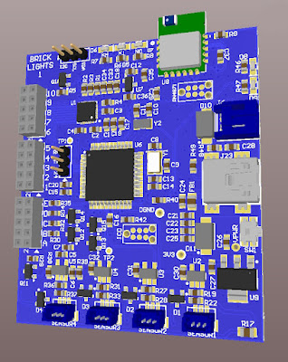
First for Brick Lights 1, I changed the board to eliminate the individual connectors for each LED that used the very small two pin connectors, the working proto is shown here. 

I used the 2mm header (2 x 5) that I used in the Brick Buddy 3.    I also changed the BT module to the smaller RN4871.  This also allowed for the board dimensions to shrink 8mm.  This is the new layout.


The first picture is the device that I am using for the development, while I wait for the new PCBs to arrive.  I should mention that under Harmony v2, most if not all of this proto was working.  So I know that the design was good.  

After generating all the I2C components in Harmony 3, I started the process of implementing the application layer code.  While Harmony generates the drivers and middleware, you still have to implement the application layer.  That took over a day to get to the point that it would compile  and at least appeared to communicate with the I2C drivers.  This I2C implementation is interrupt driven which for the most part makes it non-blocking.  

No matter what I tried, the driver would report an I2C error when transmitting a simple command.  Trying to follow the execution path down into the driver was not yielding any useful info.  After two frustrating days, I decided to try a different approach.  I have a PIC32MX470 Curiosity board and there was an I2C EEPROM example.  Also the Curiosity board allowed me to connect my Digilent Analog Discovery device very easily.  This device has an I2C decoder built in, thus I can see the commands and the protocol to determine if it is working correctly.  While the EEPROM was responding correctly, the firmware still not see it.  Stupidity number ONE.  The comments for this example were very specific to make sure the CLICK sockets were connected with ZERO ohm resistors.  Well they were not.  The 1K resistors were just enough to screw up the PIC32 read.  Once I got the example code running, I modified it to more resemble the code flow I was using.  Now that I know this was working I could go back to the proto with some confidence.

Well still not working.  Attached the wires for SDA and SCL so  I could watch the I2C protocol exchange on the Digilent device.  First thing I see is the device address is wrong.  With a 7 bit I2C address in Harmony v2 the user was required to shift 1 bit left, but in v3 the driver does that.  Thus the device address had been all wrong.  Stupidity  number TWO.  Once this was changed the I2C exchange started to work, but would not complete.  

Side step, when I first started using TI LED Drivers, I was using the LP5569.  Then COVID and they disappeared. But I could get LP55231, and earlier version that was 90% firmware compatible, though the outputs were inverted.  THE LP55xx driver that I wrote would mostly do both, though I had not completely tested it on the LP55231 since the LP5569 became available again.  The new layout will use the LP5569.  This proto was the only device that actually had the LP55231.

Looking at the  I2C trace, I could see that the final ACK was not coming in.  After hours of research, I found that the LP55231 required a software Chip enable for some commands to work.  How this worked before I am not sure, but I decided to just move on.  I modified the startup loo.  Stupidity  number THREE.

Now the entire initialization of the  LP55231 completes and the status read back shows all the registers are where they should be, just not at reset.  I still need to check if the LEDs actually light up, but for now I have high hopes it will work.

On to the BT module.


Friday, March 24, 2023

How Not To Code


This is going to be a detailed technical post on MPLB X, XC8 PIC C compiler and how not to code a project.  Or to put it simply, how not to be stupid.

The above picture is a Curiosity HPC Development Board that I talked about in this post.  This was to help me get most of the code structure working for the Brick Buddy III as shown here.

The processor on the PCB is a PIC18F26Q71.  Fairly new, but with a very nice of features and lots of program FLASH and RAM.  But it was going to be weeks before I received one from assembly.  Thus the HPC was put into use.  Instead of putting a PIC18F26Q71 in the HPC (it does have a 28 pin socket underneath the 40 pin DIP), I chose to use the 40 pin version, a PIC18F46Q71.  The only difference between the two, besides the physical 28 pins vs 40 pins, is the PIC18F46Q71 has an extra PORT (PORT D).  

The Brick Buddy III code is a derivative of Brick Buddy II and Light Buddy II.  I have not started a project completely from scratch in a long time.  Using common libraries as I explained in this post means that only the main control loop and the hardware initialization is unique, unless there is a new peripheral of some kind.  Once I updated the initialization, I started compiling the code with the PIC18F26Q71 as the processor.  This PIC has the new I2C controller and thus there was a few days of just getting the code to compile.  During the compilation, there were multiple error messages having do with available PIC ports.  Brick Buddy II is a 44 pin device and thus has a PORT D.  All of this had to be changed to accommodate the PIC PORTS available on the PIC18F26Q71.

Once that was done I started trying to see if I could get some of the basic structure working.  This include the serial interface to the PC, the I2C EEPROM that stores configuration and scripts (which would also validate the I2C software driver for the LP5569 IC LED driver).  Finally working on the Bluetooth code for the RN4871.  This BT module is similar to the RN4020, but I am sure there will be some minor road bumps.

Once I had my standard LED heartbeat running, I moved on to the serial interface.  The PCB contains a FTDI USB to UART interface IC.  So I used one of my lab ones to connect the PC to the HPC Development Board with three jumper wires (Rx, Tx & GND).  And nothing worked.

Most PICs have a Peripheral Pin Select (PPS) module.  This allows you to move digital peripheral  features to different pins.  It is basically a large switch matrix.   Some PICs can move the peripherals to any pin while others will restrict a peripheral to a subset of the PORTS.  Thus there is code at initialization that has to be executed to move the peripheral output to the desired pin.  This is shown here

        #if defined(USE_PCB)
            INT2PPS = 0x01;         // assign INT1 to RA0
            INT0PPS = 0x08;         // assign INT0 to RB0
            U1RXPPS = 0x0B;         // assign Rx1 to RB3    --RN4871
            U2RXPPS = 0x0C;         // assign Rx2 to RB4    --Console
            I2C1SCLPPS = 0x13;      // assign SCL1 to RC3        
            I2C1SDAPPS = 0x14;      // assign SDA1 to RC4

            RC3PPS = 0x20;          // assign SCL1 to RC3
            RC4PPS = 0x21;          // assign SDA1 to RC4
            RB2PPS = 0x15;          // assign Tx1 to RB2    --RN4871
            RB5PPS = 0x18;          // assign Tx2 to RB5    --Console
            RC2PPS = 0x0D;          // assign CCP1 to RC2
            RC5PPS = 0x0E;          // assign CCP2 to RC5
            RC6PPS = 0x0F;          // assign PWM1 to RC6
            RC7PPS = 0x11;          // assign PWM2 to RC7
        #elif defined(USE_DEV_BRD)
            INT2PPS = 0x15;         // assign INT1 to RC5
            INT0PPS = 0x0C;         // assign INT0 to RB4
            U1RXPPS = 0x10;         // assign Rx1 to RC0    --RN4871     
            U2RXPPS = 0x0D;         // assign Rx2 to RB5    --Console
            //U2RXPPS = 0x19;         // assign Rx2 to RD1    --Console
            I2C1SCLPPS = 0x13;      // assign SCL1 to RC3        
            I2C1SDAPPS = 0x14;      // assign SDA1 to RC4

            RC3PPS = 0x20;          // assign SCL1 to RC3
            RC4PPS = 0x21;          // assign SDA1 to RC4
            RC1PPS = 0x15;          // assign Tx1 to RC1    --RN4871
            RD0PPS = 0x18;          // assign Tx2 to RD0    --Console
            RC2PPS = 0x0D;          // assign CCP1 to RC2
            RC5PPS = 0x0E;          // assign CCP2 to RC5
            RC6PPS = 0x0F;          // assign PWM1 to RC6
            RC7PPS = 0x11;          // assign PWM2 to RC7
            RD1PPS = 0x00;
        #endif

What this also shows is that I have a conditional compile. One version for the PCB and one for the HPC Development Board.  What I found was that UART2 Rx pin would not work on any of the PORT D pins, even though the data sheet clearly indicated that it good be moved to either PORT B or PORT D.  The UART2 Tx pin worked on any of the PORT D pins I placed it on.  I verified that there was a signal present using my Digilent Analog Discover 2 (which I highly recommend).  Thus I moved the UART2 Rx pin to PORT B and all was good.  I needed to make progress, so I moved on.  Though I did post in the Microchip Support Forum what had happened.

Well someone commented on the post.  When I read the comment, I immediately knew that person had the correct answer and I had fallen again for what I discussed a month ago in this post.  Embarrassment does not even begin to describe how I felt.

Here is the initialization code with the issue

    TRISA = 0xFF;
    TRISB = 0xFF;
    TRISC = 0xFF;
    LATA = 0;
    LATC = 0;
    ANSELA = 0x00;                //all digital
    ANSELB = 0x00;                //all digital
    ANSELC = 0x00;                //all digital
    ADCON0 = 0x00;                //A2D off
    ADCON1 = 0x00;                //+ref is Vdd and -ref is Vss
#if defined (USE_PCB)
    mLED_TRIS = OUTPUT_PIN;       // make it an output
#elif defined(USE_DEV_BRD)
    mLED_B_TRIS = OUTPUT_PIN;     // make it an output
    mLED_Y_TRIS = OUTPUT_PIN;     // make it an output
#endif
    

I had the foresight to place a conditional compile for the heartbeat LED (mLED_B & mLED_Y) to control the TRIS control for the pin.  But if you look directly above that, you will notice there is no mention of either TRISD or ANSELD.

Now TRISx controls whether the PORT pin is an input or an output.  The default is INPUT, but I always like to set them all to inputs and then let the code determine which pins are inputs and which are outputs. ANSELx controls whether the PORT is an analog input pin or a digital I/O pin.  The default is analog input pin, but again I choose to make all port pins digital I/O and then let the code set those pins that will have an analog input..  But this code fragment does not set PORT D to digital I/O and thus all the PORT D pins are analog inputs.

Now the quirk in these PICs is that a digital output (TRISx = 0) will override the analog input selection.  But a digital input will not override the analog input selection.  If you think about this, that only makes sense.  When you want an analog input ( e.g. ADC input) you will set the TRIS register to input and the ANSEL register to input.  The only setup for the processor to know that you want a digital input is the ANSEL register has to be set correctly.  So here is what the code fragment looks like now.

    // Make all digital inputs for now and let init routines set the tris bits that  need to be outputs.
    TRISA = 0xFF;
    TRISB = 0xFF;
    TRISC = 0xFF;
    LATA = 0;
    LATC = 0;
    ANSELA = 0x00;                //all digital
    ANSELB = 0x00;                //all digital
    ANSELC = 0x00;                //all digital
    ADCON0 = 0x00;                //A2D off
    ADCON1 = 0x00;                //+ref is Vdd and -ref is Vss
#if defined (USE_PCB)
    mLED_TRIS = OUTPUT_PIN;       // make it an output
#elif defined(USE_DEV_BRD)
    TRISD = 0xFF;
    LATD = 0x00;
    ANSELD = 0x00;                // all digital
    mLED_B_TRIS = OUTPUT_PIN;     // make it an output
    mLED_Y_TRIS = OUTPUT_PIN;     // make it an output
#endif


Live and learn, maybe😕


Tuesday, February 7, 2023

LIght Buddy 2 - The Build Part 2


After spending the AM looking into this, I finally found the problem.  It is and isn't my new PCB.  Above is a photo of the setup.

The absolute source of the issue is the USB battery.  But it is only doing what it was designed to do.  All USB batteries have a minimal current flow cutoff circuit designed into them with a timeout delay.   When the current drops below a preset limit, the battery turns off after the delay.  This minimizes the self discharge rate.  The silver battery in the picture is the one I use for development because it seemed to have a very low cutoff, as in it doesnt turn of as long as something is plugged in.  The LED lights indicating current charge level never went out.  Other USB batteries I have require at least two devices connected with motors and LEDs active, to stay on.  And when they shut off, they shut off completely.  But when I connected the Analog Discovery to the PCB, I found this.

Sometimes the dropout is deeper,  down to just under 2VDC and varies in time from this to about 20ms.  It also happens every 27-28 seconds, which is probably the batteries timeout.  When I switched the power source to a wall charger, all of this went away and the debugger worked without failure for over 30 minutes.  Final test was to add a 100 OHM resistor load to the USB battery using the USB power connector (PCB with red and white punch down blocks on it).  Worked the same as the wall charger.  Removing the 100 ohm resistor and it reverts back to resetting every 27-28 seconds.  

My PCB just did not draw enough current to keep the battery happy.  The USB battery would start to shutdown the voltage, the PCB would start to draw more current as the voltage decreased.  This increase in current was just enough to restart the battery.  Rinse and repeat.
 

Friday, February 3, 2023

Light Buddy 2 - Build Part 1


Part of the development time was me copying code from the PIC32 project and not getting all the code.   Then there was a mismatch in the com protocol between the PC and the PIC that had to be fixed. Again, all for the good as I develop a lot more consistent interface and infrastructure code across all of my projects.

When I moved to the PCB two things started happening that were not present on the Microchip Curiosity Development Board.  I could not buy PIC16F18326 parts and had to settle for the LF version.  Should be NO big deal, though it did force the LDO decision to a 3.3VDC version.  First every few seconds the Brown out Reset would fire.  Added code to print out the the registers that tell you what caused the reset, so I know that was it.   Once I disabled BOR, that quit happening.  But now I dont know if what the PIC was seeing is not causing other issues.  

Second the PICKIT 4 is unreliable, not sure why yet.Part of it was a poor connection to the board.  I fixed that, but it will still reset it self after a few seconds.  This is probably related to the BOR issue, just not sure how to debug this, especially if the drop out is very narrow.  Also had to upgrade XC8 and MPLAB X to 5.5, which means the 64bit version.  But as the picture shows I moved to an ICD3 to continue working.

While this PIC runs at 32MHZ max, I am pushing it when running all six LEDs in full feature mode.  I can tell the service loop is not getting around as fast by the way the LEDs react.  It may be OK, I just need more time to refine the loop.  The loop is every 100msec and that may not be enough time to service 6 LEDs.  Also the free compiler does not do a great job on speed optimization.

As an aside, several people have suggested using switches to select the LED modes.  I passed on the switches for now.  The serial port makes it much easier to develop the lighting features and provides a console feature for printf.  Though I had to finish the PC program first before I could get started on the PIC firmware.  Every time I add new features to this Windows software, the whole structure of the program slightly mutates, thus more testing for older features to make sure I did not break them.   The software is getting more structured and easier to modify, just takes time.

Tuesday, February 1, 2022

Turnout & Signal Control Firmware/PC SW (Part 2)


I am going to modify this series to include the PC software, since the PIC18F firmware and the PC software are intertwined.  In the last post on this subject, I discussed some of the startup issues of getting the firmware working with the Microchip XC8 compiler, since the C18 compiler is no longer available and issues with the PIC18F47J53 itself..  Having worked through those issues, the "bringup time" on the real PCB was reduced.  There were still several "coding issues" that had be resolved.  I had put in quite a few compiler #ifdef directives.  These blocked sections of code for the Explorer 18 Development board and the real PCB.  Obviously I could not test the real PCB sections until the PCB was available.  Mostly it was coding errors of PIC18F pins and registers.

It took a little more than a day to get the PIC18F47J53 working with the EEPROM, the MCP23S18 IO Expanders and the MRF24J40 module.  So how do I test this.  

Initial Testing

The first testing I do is timer testing.  I have debug routines written for all the basic timers. In this processor those are, Timer1, Timer3 and Timer5.  I have predefined periods of 1ms, 10ms and 25ms.  Then I toggle a GPIO pin based on this and measure the output on a scope (Analog Discovery 2 in this case).  This serves multiple purposes.  First it verifies that all of the clock calculations that are defined are correct and that the timer periods are correct.  

    /*******************************************************************/
    /********************** CLOCK DEFINITIONS **************************/
    /* this is where the clock is set for calculations elsewhere       */
    /*******************************************************************/
    #define CLOCK_FREQ 48000000
    /*********************************************************************
    * Overview: These macro returns clock frequency used in Hertz.
    ********************************************************************/
    #define GetSystemClock()                    CLOCK_FREQ
    #define SYS_CLK_FrequencySystemGet()        CLOCK_FREQ
    #define SYS_CLK_FrequencyPeripheralGet()    (SYS_CLK_FrequencySystemGet()/4)
    #define SYS_CLK_FrequencyInstructionGet()   (SYS_CLK_FrequencySystemGet()/4)
    #define FCY                                 (SYS_CLK_FrequencyInstructionGet())
    #define Fosc                                SYS_CLK_FrequencySystemGet()

Next I will toggle all the GPIO pins to make sure there are no PCB manufacturing errors and no soldering errors.  Once this is done, I can move on to functionality testing.  As you can see from the code segment below, I use #ifdef to block out the debug test routines that are located in the board initialization function.  I have found this is much easier than commenting and uncommenting lines of code. The LED toggle is used a visual cue that something is happening and the code has not "crashed".

    /*******************************************************************/
    /********************** Debug Testing ONLY**************************/
    #define EarlyDebugTesting
    #ifdef EarlyDebugTesting
        while (1)
        {
            TimerOutputTesting();
            PICPortCycle();
            SPIBus_WRITE();
            SPIBus_READ();
            GetBrdSerialNumber();
            SaveBrdSerialNumber();
            mLED_G_Toggle();
        }
    #endif
    /*******************************************************************/

At this point in testing, the PC software communicating with the PIC18F firmware is how all remaining testing is done.  I have created several "Testing Functions" in the PIC18F firmeare that are callable from the PC software.  By changing what happens in these functions, allows me to exercise the entire PC software/PIC18F firmware USB HID interface and the device feature under test.

EEPROM Testing

First tests are can I write and read back the board serial number and EUI address.  Once this was good I moved on to a much more complex operation.  This involves storing the configuration data of the PCB.  More on the features of this below.  Once that worked and I could succesfully read back the configuration, the EEPROM testing was done.  The only other thing I could have done is do write-read of all location using 0x55,0xAA and waling bits.  Something you wold do in product manufacturing environment.  But at this point, if the tests I was doing worked, this full access test would have worked also.  

IO Expander (MCP23S18) Testing

Since the EEPROM was working, the SPI bus is working.  That allows me to move on to more complex testing without having to worry about underlying issues.  I chose to write to the GPIO output registers on each of the three devices.  I write the two different bytes to each of the three devices (16 bit devices), then read them back.  Then I did some simple checking that the output pins are moving.  This was a little difficult since these are open drain outputs.  But I turned on the weak pullups on the outputs to accomplish this testing.

Track Control Testing

As I explained in Part 3, there was some concern about not having pullups on these relay controls. But the MCP23S18 pullups worked just fine.  Since the spring clamp connector was not installed yet, I used a DVOM to measure resistance between the track power feed and the track siding power connection.  As I changed the siding power state in the PC software, the DVOM either shows a short or an open.

LED Control Testing

This was similar to the track control testing, except this is controlled by PIC18F GPIO pins that turn ON/OFF an N-Channel FET.  As in the IO Expander testing, when the FET is off, the output is open drain.  Since the spring clamp connector was already installed, I successively placed a 330 ohm resistor between the 5VDC point and the seven LED pins.  Then the LED control pin either measure 5VDC or ground.

Relay Control Testing

This will be done in two parts.  Once all the circuitry is installed, I will get a turnout and connect it to the PCB and then ground to the train transformer.  Since the spring clamp connectors are not installed, I can use an appropriate size wire in the component holes to control the turnout on each of the 40 positions.  Once this is done, I install the spring clamp connectors and run the test again.  The first test is looking for cold solder joints, firmware issues and PCB manufacturing issues.  The second test is looking only for soldering issues.  The connectors are relatively expensive and hard to remove, so the first test hopefully eliminates any failures that would make the PCB unusable.

MiWi Testing

In the previous incarnation of the turnout and signal control board, I had spent a lot of time getting the MiWi to work.  Also I had done a few consulting projects that used this MiWi Mesh Protocol.  In the Explorer 18 Development board version, I used the latest non-library version that would compile under an XC8 compiler, did not want to deal with libraries.  When I turned the development board on and the current train layout, the development board connected to that MiWi network and all was good.  As described in this Blog Post, I use a Zena Device for the master station.  The PC software connects to it over a USB HID interface and then sends/receives messages to/from the multiple turnout & signal control PCBs mounted under the layout.  Most of the testing above is done using this PC interface and sending/receiving MiWi messages across the network.  While this may not be a comprehensive test, bit error rate, messages dropped, etc, it is good enough for what I am trying to do.

In the next part I will describe the PC software in more detail and some of the issues that had to be resolved as well as others that may not be solved yet.


Monday, January 31, 2022

Train Turnout & Signal Control Design (Part 4)


I have discussed the PCB development in these previous posts, Part 1 , Part 2, and Part3. Here you can see the PCB with most of the components installed.  Only components missing now are the spring clamp connectors and the FETs circuit that drives the 40 relay contacts.

When I built the original PCBs, I only really tested the relay interface.  The track and LED control were only partially implemented in the PIC18F firmware.  Now I am getting more done and have actually tested the track and LED control interfaces and they work as expected.  Since all the relays were installed along with the LED control circuits, I have had the opportunity to test these as well.  Found one cold solder joint, but other than that, all was good.

One item I have not brought up is the small daughter card plugged in perpendicular on the left hand side.  This is a substitute for the MRF24J40MA module from Microchip. This is a Digilent Pmod device (similar to Mikroe Click Boards).  I added a connector for this Pmod board when it became quite obvious buying Microchip MRF24J40MA modules at a reasonable price was going to be impossible.  This PmodRF2 is an excellent temporary substitute for the Microchip module.  I was able to purchase them at Digikey, Mouser and Amazon, so I picked up 6 of them just to have them.  I prefer the Microchip Module since it is soldered down. When the PCB is installed underneath the train layout, this daughter card will be perpendicular to the bottom of the layout.  Underneath the layout will become storage and I am afraid that these cards will get bumped into and either destroy them or the entire PCB.  But for now they are better than nothing.


Sunday, January 30, 2022

Train Turnout & Signal Control Design (Part 3)


I have discussed the PCB development in these previous posts, Part 1 and Part 2. Here you can see the PCB with the power section installed and the PCB running from a train transformer.


The parts that I received from WinSource work just fine.  They were about 2X the Digikey price and $50 DHL charge, put I have parts.  This design uses the LMR14030, which has a 40V input maximum and a 3A output @5VDC.  The 5VDC has three uses

  • Power the digital section through the MCP1825ST 3.3VDC LDO
    • PIC18F47J53, MRF24J40MA, MCP23S18, 24LC160
    • The above use just under 75mA
  • Provide miscellaneous power,
    •  the bias control for the switch/signal relays and power the track control relays
    • This section uses < 10mA, on average
  • LED power for the 7 LED channels
    • This is where most of the 5VDC will be consumed.
    • Probably about 60mA per channel or <500mA

This leads to a total power consumption number of less than 600mA.   So the LMR14030 is a little over kill.  The other two designs, the MiWi to BT Bridge and the Train LED Controller, both use the LMR140100.  This DC-DC converter is from the same family as the LMR14030, but has a maximum current output of 1A, a small reduction in PCB real estate and smaller simpler package to install (no power pad).  If an LMR14010 had been used, the total LED power would have been limited to about 850-900mA.  At a max of 20mA per LED attached, this would provide power for about 40 to 50 LEDs.  With 4 to 5 of these installed and the Train LED Controller, that would have been sufficient. 

Not sure how noisy this DC-DC is, but the USB connected without issues.  I then reinstalled the MiWi code and the entire system connected to the MiWi network.  There are some obvious protocol issues that need to be resolved.  I need to get my TEK scope out to look at the noise factor.  The Analog Discovery 2 is nice, but it has limits when looking at power supply noise.

The MCP23S18 IO expanders have open drain outputs.  I turned this into an advantage with the switch/signal relay control.  Instead of 3.3VDC to turn on the controlling FETs, I designed a way for 5VDC to be used to turn the FETs on, driving them further into saturation and providing a little more current to drive the relays.  There are 3 of these MCP23S18 16 bit IO expanders.  Of the 48 ports, 40 are used for switch/signal relay control.  The remaining 8 are used to control 4 track/catenary control relays (Track ON/Track OFF).  These are used to control the track/catenary power to dead end track sidings.  This provides the ability to park engines and not worry about power being applied to them, especially in the non-digital mode of train operation.  

In my haste to get this board done before Chinese New Year holiday, I missed that the control lines to the FETs controlling these track/catenary relays did not have pullup resistors. Oops😒.  Well the MCP23S18 does have weak builtin pullups that are firmware controlled.  I was worried that they might be to weak to turn the FETs on.  Fortunately the FETs require very little current to turn on and the track/catenay control relays work just fine.

Next is to work on the protocol issues and install the 40 FETs/diodes/resistors that control the switch/signal relays. 


Friday, January 28, 2022

Train Turnout & Signal Control Design (Part 2)


I received the PCB the other day.  I had discussed the design ideas for this PCB in Part 1.The request was for yellow solder mask with black silkscreen.  As you can see from the picture above, it is more orange than yellow.  I think there was too much RED left in the solder mask machine when they applied the yellow.  Oh well it is different and the price for a 4 layer was still very good.  Hopefully there wont be any other problems with the PCB.

Here is the digital part working.

All of the digital uses 3.3VDC.  The power section takes 16VAC (train layout voltage) and generates 20VDC+ (straight out of the full wave bridge with some capacitance) for activating the turnout/signal relays and then generates 5VDC (for LEDs and relay bias control) with a small DC-DC converter.  The 3.3VDC is generated from a small LDO.  Look close to the right of the push button and below the jumper and you can see a space wired SOT23 device.  The LDO was supposed to be a SOT223-3 device.  My first choice was a MCP1825ST, but was out in time to next Xmas, so I found what I thought was a pin compatible LDO, it wasn't.   Now I have found one (triple check), but I thought I would wait a few more days to see if anything else needs replacing. 

The jumper selects either the Power Section 5VDC or VUSB.  That way I can power the digital section without the train transformer and still do debugging and programming.  The Analog Discovery 2 from Diligent is helpful when looking at changing outputs.  With the 34" monitor, I can run a remote desktop window for my other laptop which is running the Digilent Waveforms and the PC program that interfaces to the PCB.  The main laptop has the MPLABX and ICD connection. 

Next up is the power section.  The DC-DC converters came in today, we will see if the Asia reseller market has real parts.


Thursday, January 13, 2022

Turnout & Signal Control Firmware (Part 1)


In the last post I described one of the changes I did to this design and how I improved  the relay control.  I have been using an old Explorer 18 dev board to rebuild the firmware for the train control using the XC8 compiler instead of the old C18 compiler.  The C18 is not available anymore and occasionally there is need for the higher optimization than what the  free mode provides.  The Explorer 18  allows me to use a plugin module with a PIC8F47J53 instead of the processor soldered to the board.  This is the processor that is use for the train control design.

This design requires PPS for moving features to specific pins.  The second SPI port and few other peripherals are only available through PPS.   Due to traffic on the MiWi network, the MRF24J40MA module prefers it's own SPI port.  The second SPI port is used for the I/O expanders (MCP23S18) and the EEPROM that contains the network and train control configuration.  (The 18F47J53 has no local EEPROM and I dont like using PIC flash unless there is no choice, not enough usable cycles.)  I still had the plugin I built for the Explorer 18 that had the MiWi module on it and an EEPROM.

After re-documenting the plugin correctly, I was able to read and write to the EEPROM in a small debug section at the beginning of the program.  (I am using the Analog Discovery 2 to monitor the SPI bus.  Glad I bought that!)  However when running the whole program, the EEPROM read would eventually fail later on in the program.  I could read basic info at the beginning of the program, but once the MiWi network connected, it would fail to read.  The SPI bus showed the EEPROM CS going active, but no clock.

Debugging this became quite fun, since all the EEPROM reads went through one function, but the breakpoints would eventually cause Windows to disconnect the USB and thus I would loose control of the program.   The code where the MiWi network is accessing the EEPROM is buried in a library, which made it all the more fun.

I had assumed that once PPS was selected, all other functions were overridden.   After two days of debugging, I came to the conclusion that this was obviously not true.

Here is what is on RC1
RC1      standard I/O pin
CCP8     capture/compare I/O
T1OSI    Timer1 osc input
UOE      USB UOE output
RP12     PPS pin

The capture/compare feature was turned off, Timer1 was set to internal instruction clock and UOE is a configuration bit option, so this cant be altered by code.  At various run points, none of this changed.  Then I found this little tidbit in the Timer 1 section

"When Timer1 is enabled, the RC1/CCP8/T1OSI/UOE/RP12 and RC0/T1OSO/T1CKI/RP11 pins become inputs. This means the values of TRISC<1:0> are ignored and the pins are read as ‘0’."

Well this can't be true, because this worked on the original design, so something else is going on.  Then I found this footnote:

"The Timer1 oscillator crystal driver is powered whenever T1OSCEN (T1CON<3>) or T3OSCEN (T3CON<3>) = 1. The circuit is enabled by the logical OR of these two bits. When disabled, the inverter and feedback resistor are disabled to eliminate power drain. The TMR1ON and TMR3ON bits do not have to be enabled to power up the crystal driver."

This is where cut and paste gets you and Microchip Tech Docs staff is guilty as anyone is.  The PIC18F47J53 actually has 8 timers, and Timer3 and Timer5 are identical.  For some reason the MiWi library wanted T1OSCEN set,which turned on the crystal driver.  The note implies that this only applies to T1OSCEN and T3OSCEN, when in reality it is the logical OR of T1 or T3 or T5 OSCEN as shown in the Timer schematic in the data sheet.  And then somehow T5OSCEN also was set. Timer 3/5 section additionally explains that this processor has the capability to switch to the Timer1 OSC as a clock source and this mode can turn the crystal driver on also.  Fortunately this is not used that I can find, but I have put in a forced write for this register.

When ensuring that all these bits are in the proper state, the result is a stable system and the Explorer 18 connecting to the MiWi network in the train room.  Still need to verify that all the data transfers are working, but that is much simpler than finding this.

On to the next task