Monday, January 31, 2022

Train Turnout & Signal Control Design (Part 4)


I have discussed the PCB development in these previous posts, Part 1 , Part 2, and Part3. Here you can see the PCB with most of the components installed.  Only components missing now are the spring clamp connectors and the FETs circuit that drives the 40 relay contacts.

When I built the original PCBs, I only really tested the relay interface.  The track and LED control were only partially implemented in the PIC18F firmware.  Now I am getting more done and have actually tested the track and LED control interfaces and they work as expected.  Since all the relays were installed along with the LED control circuits, I have had the opportunity to test these as well.  Found one cold solder joint, but other than that, all was good.

One item I have not brought up is the small daughter card plugged in perpendicular on the left hand side.  This is a substitute for the MRF24J40MA module from Microchip. This is a Digilent Pmod device (similar to Mikroe Click Boards).  I added a connector for this Pmod board when it became quite obvious buying Microchip MRF24J40MA modules at a reasonable price was going to be impossible.  This PmodRF2 is an excellent temporary substitute for the Microchip module.  I was able to purchase them at Digikey, Mouser and Amazon, so I picked up 6 of them just to have them.  I prefer the Microchip Module since it is soldered down. When the PCB is installed underneath the train layout, this daughter card will be perpendicular to the bottom of the layout.  Underneath the layout will become storage and I am afraid that these cards will get bumped into and either destroy them or the entire PCB.  But for now they are better than nothing.


Sunday, January 30, 2022

Train Turnout & Signal Control Design (Part 3)


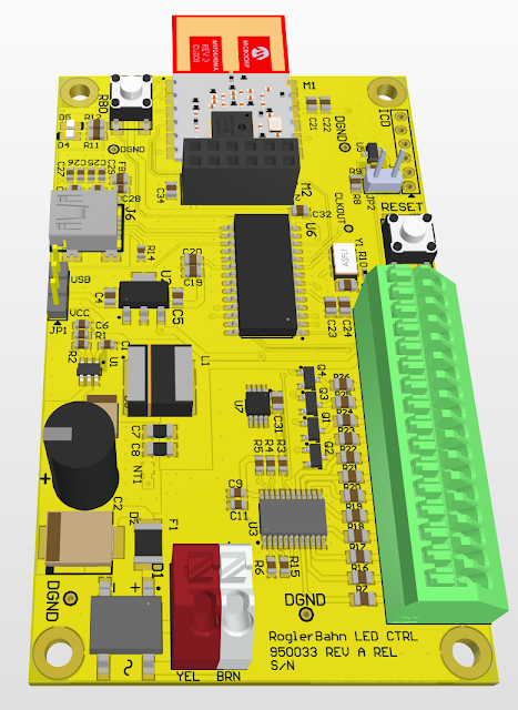
I have discussed the PCB development in these previous posts, Part 1 and Part 2. Here you can see the PCB with the power section installed and the PCB running from a train transformer.


The parts that I received from WinSource work just fine.  They were about 2X the Digikey price and $50 DHL charge, put I have parts.  This design uses the LMR14030, which has a 40V input maximum and a 3A output @5VDC.  The 5VDC has three uses

  • Power the digital section through the MCP1825ST 3.3VDC LDO
    • PIC18F47J53, MRF24J40MA, MCP23S18, 24LC160
    • The above use just under 75mA
  • Provide miscellaneous power,
    •  the bias control for the switch/signal relays and power the track control relays
    • This section uses < 10mA, on average
  • LED power for the 7 LED channels
    • This is where most of the 5VDC will be consumed.
    • Probably about 60mA per channel or <500mA

This leads to a total power consumption number of less than 600mA.   So the LMR14030 is a little over kill.  The other two designs, the MiWi to BT Bridge and the Train LED Controller, both use the LMR140100.  This DC-DC converter is from the same family as the LMR14030, but has a maximum current output of 1A, a small reduction in PCB real estate and smaller simpler package to install (no power pad).  If an LMR14010 had been used, the total LED power would have been limited to about 850-900mA.  At a max of 20mA per LED attached, this would provide power for about 40 to 50 LEDs.  With 4 to 5 of these installed and the Train LED Controller, that would have been sufficient. 

Not sure how noisy this DC-DC is, but the USB connected without issues.  I then reinstalled the MiWi code and the entire system connected to the MiWi network.  There are some obvious protocol issues that need to be resolved.  I need to get my TEK scope out to look at the noise factor.  The Analog Discovery 2 is nice, but it has limits when looking at power supply noise.

The MCP23S18 IO expanders have open drain outputs.  I turned this into an advantage with the switch/signal relay control.  Instead of 3.3VDC to turn on the controlling FETs, I designed a way for 5VDC to be used to turn the FETs on, driving them further into saturation and providing a little more current to drive the relays.  There are 3 of these MCP23S18 16 bit IO expanders.  Of the 48 ports, 40 are used for switch/signal relay control.  The remaining 8 are used to control 4 track/catenary control relays (Track ON/Track OFF).  These are used to control the track/catenary power to dead end track sidings.  This provides the ability to park engines and not worry about power being applied to them, especially in the non-digital mode of train operation.  

In my haste to get this board done before Chinese New Year holiday, I missed that the control lines to the FETs controlling these track/catenary relays did not have pullup resistors. Oops😒.  Well the MCP23S18 does have weak builtin pullups that are firmware controlled.  I was worried that they might be to weak to turn the FETs on.  Fortunately the FETs require very little current to turn on and the track/catenay control relays work just fine.

Next is to work on the protocol issues and install the 40 FETs/diodes/resistors that control the switch/signal relays. 


Friday, January 28, 2022

Train Turnout & Signal Control Design (Part 2)


I received the PCB the other day.  I had discussed the design ideas for this PCB in Part 1.The request was for yellow solder mask with black silkscreen.  As you can see from the picture above, it is more orange than yellow.  I think there was too much RED left in the solder mask machine when they applied the yellow.  Oh well it is different and the price for a 4 layer was still very good.  Hopefully there wont be any other problems with the PCB.

Here is the digital part working.

All of the digital uses 3.3VDC.  The power section takes 16VAC (train layout voltage) and generates 20VDC+ (straight out of the full wave bridge with some capacitance) for activating the turnout/signal relays and then generates 5VDC (for LEDs and relay bias control) with a small DC-DC converter.  The 3.3VDC is generated from a small LDO.  Look close to the right of the push button and below the jumper and you can see a space wired SOT23 device.  The LDO was supposed to be a SOT223-3 device.  My first choice was a MCP1825ST, but was out in time to next Xmas, so I found what I thought was a pin compatible LDO, it wasn't.   Now I have found one (triple check), but I thought I would wait a few more days to see if anything else needs replacing. 

The jumper selects either the Power Section 5VDC or VUSB.  That way I can power the digital section without the train transformer and still do debugging and programming.  The Analog Discovery 2 from Diligent is helpful when looking at changing outputs.  With the 34" monitor, I can run a remote desktop window for my other laptop which is running the Digilent Waveforms and the PC program that interfaces to the PCB.  The main laptop has the MPLABX and ICD connection. 

Next up is the power section.  The DC-DC converters came in today, we will see if the Asia reseller market has real parts.


Thursday, January 20, 2022

Train LED Controller


I completed my last design for a while.  This is the LED controller for the lights in the buildings, freight yards, etc.   It has 12 LED channels, 8 of them are controlled by an I2C based LED controller and 4 by the PIC.  The 4 PIC channels are connected to PWM channels and the LED controller has individual PWM controllers for each of the 8 channels.  This will allow for some different lighting effects besides just off and on.

This uses the PIC18F27J53 processor and a MRF24J40MA MiWi transceiver.  As I have done with the switch/signal board, I also included a connector for the PMOD version of this.  I have several of those and will have to use them until the MiWi Module becomes available from other than the resellers.

This was done on Sunday, but during the final purchase review I discovered that the LED controller I picked did not do everything I wanted.  I had discovered a LED controller (LP5569) from TI when working on the new Brick Controller design.  It was a 9 channel (triple RGB) sink style controller, but with a current limit of 25mA that was software controlled.  That was OK for a Lego display and might have worked for the train.  But that IC disappeared, with next availability sometime in 2023.  I found a firmware compatible earlier version (LP55231) at a Chinese reseller so I bought the MOQ qty of 20, but at 5x the price.  This new LED controller is a source style, 25mA limit.  After much thought on how this PCB would be used in layout lighting, I decided that 25mA was too much of a restriction and in the end did not like the source style.  I had considered placing a N channel FET in each channel to increase the current limit, but that just seemed like adding a lot of complexity.

So after a day of searching for alternatives that can be purchased, I found one from NXP.  This is an 8 channel sink style controller, each channel can sink 100mA.  The TI controller was in nice compact 24 pin QFN with a big power pad on the bottom.  The NXP is in a 24 TSSOP package, though it has 4 ground pins.  We will see how it handles lots of current.  This NXP does come in a QFN, but it is being discontinued.  I had to give up the RGB feature of the LP5569/LP55231, but I have not found an application for that feature yet.

This design has a DC-DC converter that converts the 16VAC to 5VDC @ 1A+.  The processor and the radio use about 50mA, so the rest is dedicated to lighting power.  It also has 8K or bigger I2C EEPROM for storing the lighting configuration, so on power up a standard lighting arrangement will be executed.  I wanted to use a SPI EEPROM, since the other two boards use those.  But the PIC18F27J53 has 2 MSSP devices, but has only one I2C port and it is fixed (electrical requirements of I2C dont allow for reassignment) and uses the same pins as the fixed SPI port.  So when you use an I2C port on this part, you loose a SPI port.  Since the radio module wants to be on its own SPI port and the LED controller needs an I2C port, the EEPROM became I2C.  Which created its own availability nightmare.  Mostly finding an IC package and industry standard firmware access I might be able to buy in the future.


Wednesday, January 19, 2022

A MiWi to Bluetooth Bridge


To control the train system I used the Zena Wireless Adapter, pictured below from Microchip.  The Zena has a PIC18F27J53 and the MRF24J40 MiWi transceiver.  I actually opened it up and reprogrammed it so it would handle by higher level protocols.  One big downside is even with a USB Bootloader, you still have to open it up.  Also I am constantly misplacing it, since it is just a USB dongle.

AC182015-1 Microchip Technology | Mouser

I also would like to use the Tablet/Phone to control the trains.  This means either a MiWi-Wifi bridge or a MiWi-Bluetooth bridge.  I bought the Microchip developers kit for the Wifi bridge, but I have never figured out to do these micro web servers, etc.  With Bluetooth I have extensive libraries, since I use it for quite a few of my little modules.  So the picture at the top of this post is the answer.  This PCB will be mounted on the edge of the train layout so that I can connect a USB cable when needed.

What is it?

The design is quite simple,  A 2" x 4" 2 layer board that is everything the Zena is plus a BT module and some LED power.  Since you cant buy MRF24J40MA modules until late 2022/early 2023, I decide to go a slightly different route.  I can buy the Mikro Bus CLICK versions (https://www.mikroe.com/mikrobus).  On some level just plugging in a module is appealing,  I did violated the Mikro Bus spec by only connecting the lines I need and in my configuration.  But the configuration seems to be the same for all the MiWi and BT Click modules.  Thus you will be able to use this PCB to build a bridge between any MiWi module (2.4GHz, 900Mhz and 315Mhz) and any BT device that a CLICK module exists for. 

This design has a DC-DC converter that converts the 16VAC to 5VDC @ 1A+, but is good up to 24VAC input.  The processor and the radios use about 50mA, so the rest is dedicated to lighting power.  I added a SPI EEPROM for storing configuration information. Finally there is a 5VDC switch that will be used for 5VDC LED lighting, using the left Red/White connector.  There is about 800mA+ of excess power.

This one is supposed to be white with black silkscreen, the color rendered did not quite do white, it was 255, 255, 255 though.


Thursday, January 13, 2022

Turnout & Signal Control Firmware (Part 1)


In the last post I described one of the changes I did to this design and how I improved  the relay control.  I have been using an old Explorer 18 dev board to rebuild the firmware for the train control using the XC8 compiler instead of the old C18 compiler.  The C18 is not available anymore and occasionally there is need for the higher optimization than what the  free mode provides.  The Explorer 18  allows me to use a plugin module with a PIC8F47J53 instead of the processor soldered to the board.  This is the processor that is use for the train control design.

This design requires PPS for moving features to specific pins.  The second SPI port and few other peripherals are only available through PPS.   Due to traffic on the MiWi network, the MRF24J40MA module prefers it's own SPI port.  The second SPI port is used for the I/O expanders (MCP23S18) and the EEPROM that contains the network and train control configuration.  (The 18F47J53 has no local EEPROM and I dont like using PIC flash unless there is no choice, not enough usable cycles.)  I still had the plugin I built for the Explorer 18 that had the MiWi module on it and an EEPROM.

After re-documenting the plugin correctly, I was able to read and write to the EEPROM in a small debug section at the beginning of the program.  (I am using the Analog Discovery 2 to monitor the SPI bus.  Glad I bought that!)  However when running the whole program, the EEPROM read would eventually fail later on in the program.  I could read basic info at the beginning of the program, but once the MiWi network connected, it would fail to read.  The SPI bus showed the EEPROM CS going active, but no clock.

Debugging this became quite fun, since all the EEPROM reads went through one function, but the breakpoints would eventually cause Windows to disconnect the USB and thus I would loose control of the program.   The code where the MiWi network is accessing the EEPROM is buried in a library, which made it all the more fun.

I had assumed that once PPS was selected, all other functions were overridden.   After two days of debugging, I came to the conclusion that this was obviously not true.

Here is what is on RC1
RC1      standard I/O pin
CCP8     capture/compare I/O
T1OSI    Timer1 osc input
UOE      USB UOE output
RP12     PPS pin

The capture/compare feature was turned off, Timer1 was set to internal instruction clock and UOE is a configuration bit option, so this cant be altered by code.  At various run points, none of this changed.  Then I found this little tidbit in the Timer 1 section

"When Timer1 is enabled, the RC1/CCP8/T1OSI/UOE/RP12 and RC0/T1OSO/T1CKI/RP11 pins become inputs. This means the values of TRISC<1:0> are ignored and the pins are read as ‘0’."

Well this can't be true, because this worked on the original design, so something else is going on.  Then I found this footnote:

"The Timer1 oscillator crystal driver is powered whenever T1OSCEN (T1CON<3>) or T3OSCEN (T3CON<3>) = 1. The circuit is enabled by the logical OR of these two bits. When disabled, the inverter and feedback resistor are disabled to eliminate power drain. The TMR1ON and TMR3ON bits do not have to be enabled to power up the crystal driver."

This is where cut and paste gets you and Microchip Tech Docs staff is guilty as anyone is.  The PIC18F47J53 actually has 8 timers, and Timer3 and Timer5 are identical.  For some reason the MiWi library wanted T1OSCEN set,which turned on the crystal driver.  The note implies that this only applies to T1OSCEN and T3OSCEN, when in reality it is the logical OR of T1 or T3 or T5 OSCEN as shown in the Timer schematic in the data sheet.  And then somehow T5OSCEN also was set. Timer 3/5 section additionally explains that this processor has the capability to switch to the Timer1 OSC as a clock source and this mode can turn the crystal driver on also.  Fortunately this is not used that I can find, but I have put in a forced write for this register.

When ensuring that all these bits are in the proper state, the result is a stable system and the Explorer 18 connecting to the MiWi network in the train room.  Still need to verify that all the data transfers are working, but that is much simpler than finding this.

On to the next task

Wednesday, January 12, 2022

Train Turnout & Signal Control Design (Part 1)


As I continue to work on the train layout, one thing I am realizing is that I dont have enough turnout and signal control boards from the previous build 10 years ago.  That design had a few issues and was more complicated than it needed to be.  So I did an update, corrected a few errors, made changes for parts that are not available right now and simplified the design.  

One big change was driving the relays in the turnouts and signals.  I need to drive relays in the turnouts/signals for 100ms to 400ms, depending on the type, and only one at a time is ever activated.  

The first issue is providing enough drive to fully turn on the FET, thus lowering Rds and reducing heat.  With 3.3VDC that can be problematic depending on the FET.  I need flexibility in buying so I am wanting to use 5VDC.  The MSP23S8 I/O Expander has to run at 3.3V, because the interface to the PIC runs only at 3.3V.  But the I/O expander has open drain outputs good to 5.5VDC, so it seems attaching a pull-up resistor to 5VDC will improve my drive problem, since a Vgs of 5V will fully turn on most of these FETs.

The next issue is at startup when nothing is defined.  The MSP23S18 I/O pins are inputs on reset, which will float the GATE of the driving FET.  If the BIAS point (see schematic) is connected to 5VDC, then until the MSP23S18 is programmed and all of the outputs are set to zero, all of the FETs will be on.   This will not be good for the relays as the relays in a turnout will be fighting each other.  So I came up with an idea of a BIAS control.  A single FET connected to a PIC I/O pin.  This  will hopefully do the following:

On POR:  RB0 will be an input, Rin will turn the FET on enough to drive the BIAS point to GND.  This should turn off all the relay FETs and everything will be stable. 
Initialization:  Once RB0 is set as an output it will be set high, to keep the BIAS point at GND while the MSP23S18 is initialized for the outputs to be all ZERO.
Finally:  Once the MSP23S18 is initialized, then RB0 can set to ZERO, which will change the BIAS point to 5VDC.  

Below is a reduced schematic of how this will be done.